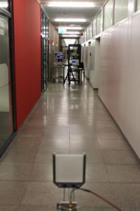
Extension of cable-based telecommunication networks requires high investments in both conurbations and rural areas. Broadband data transmission via radio relay links might help to cross rivers, motorways or nature protection areas at strategic node points, and to make network extension economically feasible. In the current issue of the nature photonics magazine, researchers present a method for wireless data transmission at a world-record rate of 100 gigabits per second. (doi: 10.1038/nphoton.2013.275) In their record experiment, 100 gigabits of data per second were transmitted at a frequency of 237.5 GHz over a distance of 20 m in the laboratory. In previous field experiments under the “Millilink” project funded by the BMBF, rates of 40 gigabits per second and transmission distances of more than 1 km were reached. For their latest world record, the scientists applied a photonic method to generate the radio signals at the transmitter. After radio transmission, fully integrated electronic circuits were used in the receiver. Setup for the world record of wireless data transmission at 100 gigabits per second: The receiver unit (left)
 |
| Photo: KI |
receives the radio signal that is recorded by the oscilloscope (right). “Our project focused on integration of a broadband radio relay link into fiber-optical systems,” Professor Ingmar Kallfass says. He coordinated the “Millilink” project under a shared professorship funded by the Fraunhofer Institute for Applied Solid State Physics (IAF) and the Karlsruhe Institute of Technology (KIT). Since early 2013, he has been conducting research at Stuttgart University. “For rural areas in particular, this technology represents an inexpensive and flexible alternative to optical fiber networks, whose extension can often not be justified from an economic point of view.” Kallfass also sees applications for private homes: “At a data rate of 100 gigabits per second, it would be possible to transmit the contents of a blue-ray disk or of five DVDs between two devices by radio within two seconds only.” In the laboratory experiment, radio relay transmission has covered a distance of up to 20 m already. In the experiments, latest photonic and electronic technologies were combined: First, the radio signals are generated by means of an optical method. Several bits are combined by so-called data symbols and transmitted at the same time. Upon transmission, the radio signals are received by active integrated electronic circuits. The transmitter generates the radio signals by means of an ultra-broadband so-called photon mixer made by the Japanese company NTT-NEL. For this, two optical laser signals of different frequencies are superimposed on a photodiode. An electrical signal results, the frequency of which equals the frequency difference of both optical signals, here, 237.5 GHz. The millimeter-wave electrical signal is then radiated via an antenna. “It is a major advantage of the photonic method that data streams from fiber-optical systems can directly be converted into high-frequency radio signals,” Professor Jürg Leuthold says. He proposed the photonic extension that was realized in this project. The former head of the KIT Institute of Photonics and Quantum Electronics (IPQ) is now affiliated with ETH Zurich. “This advantage makes the integration of radio relay links of high bit rates into optical fiber networks easier and more flexible.“ In contrast to a purely electronic transmitter, no intermediate electronic circuit is needed. “Due to the large bandwidth and the good linearity of the photon mixer, the method is excellently suited for transmission of advanced modulation formats with multiple amplitude and phase states. This will be a necessity in future fiber-optical systems,” Leuthold adds. Reception of radio signals is based on electronic circuits. In the experiment, a semiconductor chip was employed that was produced by the Fraunhofer Institute of Applied Solid State Physics (IAF) within the framework of the “Millilink” project. The semiconductor technology is based on high-electron-mobility transistors (HEMT) enabling the fabrication of active, broadband receivers for the frequency range between 200 and 280 GHz. The integrated circuits have a chip size of a few square millimeters only. The receiver chip can also cope with advanced modulation formats. As a result, the radio link can be integrated into modern optical fiber networks in a bit-transparent way. Already in May this year the team succeeded in transmitting a data rate of 40 gigabits per second over a long distance in the laboratory using a purely electronic system. In addition, data were transmitted successfully over a distance of one kilometer from one high-riser to another in the Karlsruhe City center. “The long transmission distances in “Millilink” were reached with conventional antennas that may be replaced by fully integrated miniaturized antenna designs in future compact systems for indoor use,” says Professor Thomas Zwick, Head of the KIT Institut für Hochfrequenztechnik und Elektronik (Institute of High-Frequency Technology and Electronics). The present data rate can be still increased. “By employing optical and electrical multiplexing techniques, i.e., by simultaneously transmitting multiple data streams, and by using multiple transmitting and receiving antennas, the data rate could be multiplied,” says Swen König from the KIT Institute of Photonics and Quantum Electronics (IPQ), who conceived and conducted the recent world-record experiment. “Hence, radio systems having a data rate of 1 terabit per second appear to be feasible.” The “Millilink” project (March 2010 to May 2013) was funded with a total budget of EUR 2 million by the Federal Ministry of Education and Research (BMBF) under the program “Broadband Access Networks of the Next Generation”. Apart from the research institutions of Fraunhofer IAF and KIT, the industry partners Siemens AG, Kathrein KG, and Radiometer Physics GmbH participated in the project. The project focused on integrating wireless or radio links into broadband optical communication networks for rapid internet access in rural areas in particular. Other possible applications are indoor wireless local area networks (WLAN), wireless personal area networks (WPAN), and intra-machine and board-to-board communication. In the recent experiment, the originally purely electronic “Millilink” concept was extended by a photonic transmitter. At KIT, work is now continued under the Helmholtz International Research School of Teratronics (HIRST), a graduate school focusing on the combination of photonic and electronic methods for signal processing at highest frequencies. Contacts and sources:
Monika Landgraf.
Helmholtz Association Reference: Wireless sub-THz communication system with high data rate. S. Koenig, D. Lopez-Diaz, J. Antes, F. Boes, R. Henneberger, A. Leuther, A. Tessmann, R. Schmogrow, D. Hillerkuss, R. Palmer, T. Zwick, C. Koos, W. Freude, O. Ambacher, J. Leuthold, and I. Kallfass. nature photonics. doi: 10.1038/nphoton.2013.275, http://www.nature.com/nphoton/index.html. Karlsruhe Institute of Technology (KIT) is a public corporation according to the legislation of the state of Baden-Württemberg. It fulfills the mission of a university and the mission of a national research center of the Helmholtz Association. Research activities focus on energy, the natural and built environment as well as on society and technology and cover the whole range extending from fundamental aspects to application. With about 9000 employees, including nearly 6000 staff members in the science and education sector, and 24000 students, KIT is one of the biggest research and education institutions in Europe. Work of KIT is based on the knowledge triangle of research, teaching, and innovation.
Source: Nano Patents And Innovation